← VW Polo 6N2 Wiring Diagram: The Hatchback Electrical Guide vw id.2 kommt als suv: volkswagen kündigt neues elektroauto an Transform Your Space With Inspirational Wall Decor and Captivating Captions 【亲测能用】c4d greyscale gorilla出品动画插件:transform v1.2254下载-3d溜溜网 →
If you are looking for PCB厂:基于Cadence的高速PCB设计分享 - 鑫景福科技 you've visit to the right web. We have 25 Pictures about PCB厂:基于Cadence的高速PCB设计分享 - 鑫景福科技 like PCB Trace: The Backbone of Modern Circuit Design, PCB Meaning in Electronics | Video& Image& Text Explanation and also PCB Assembly UK | PCBA | ABL Circuits. Read more:
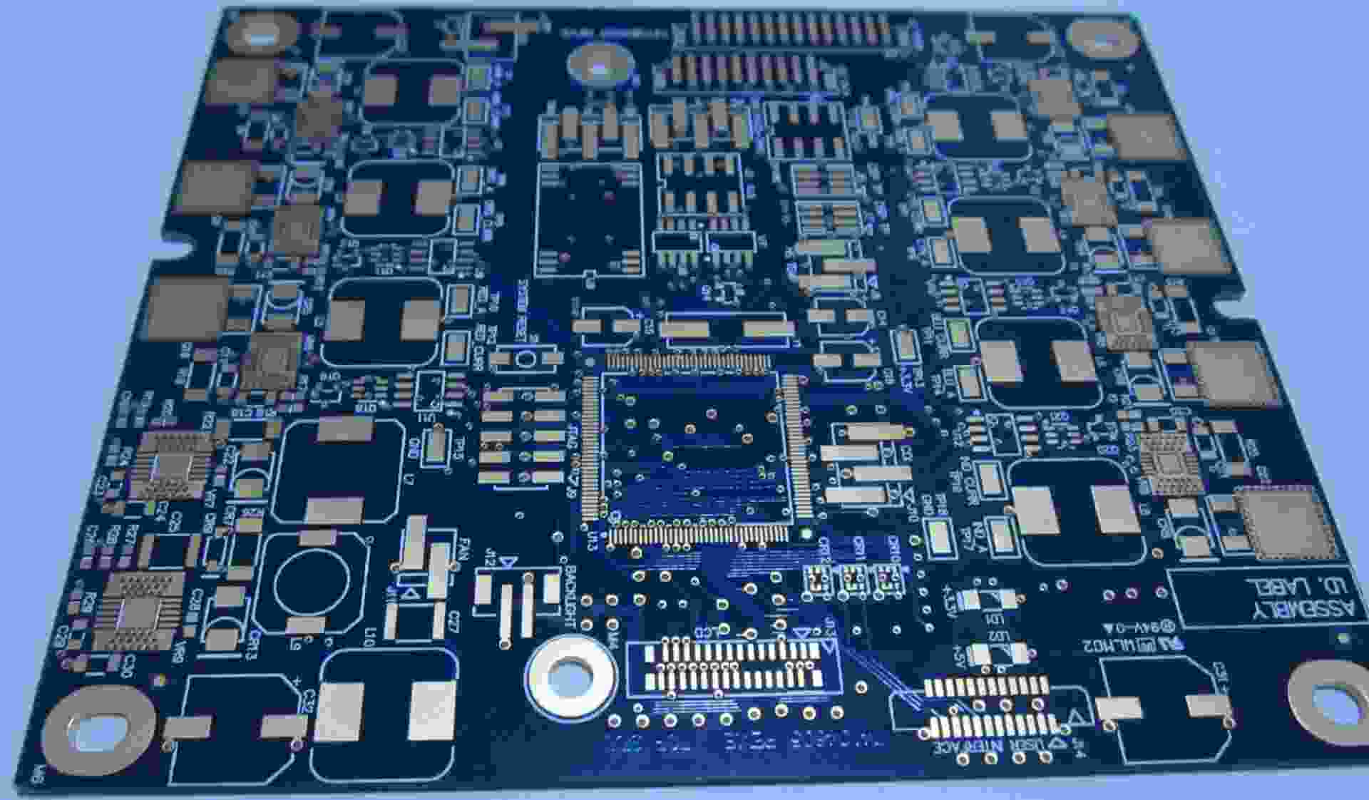
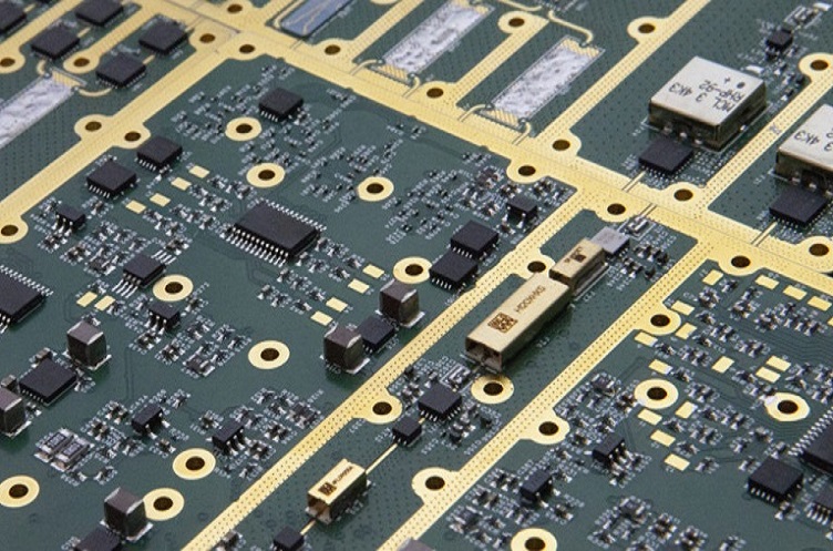
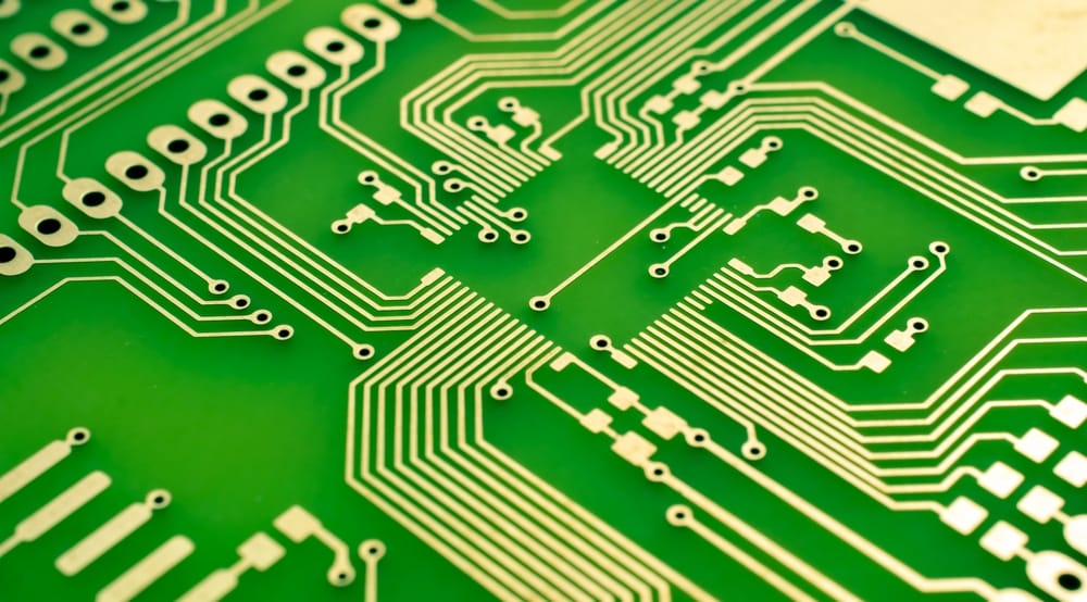
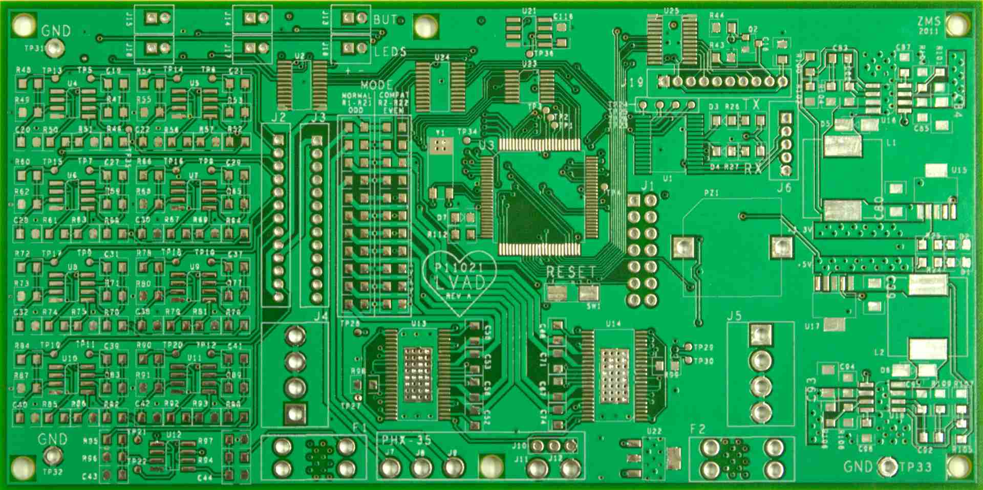
PCB厂:基于Cadence的高速PCB设计分享 - 鑫景福科技
 www.kingfordpcb.cn
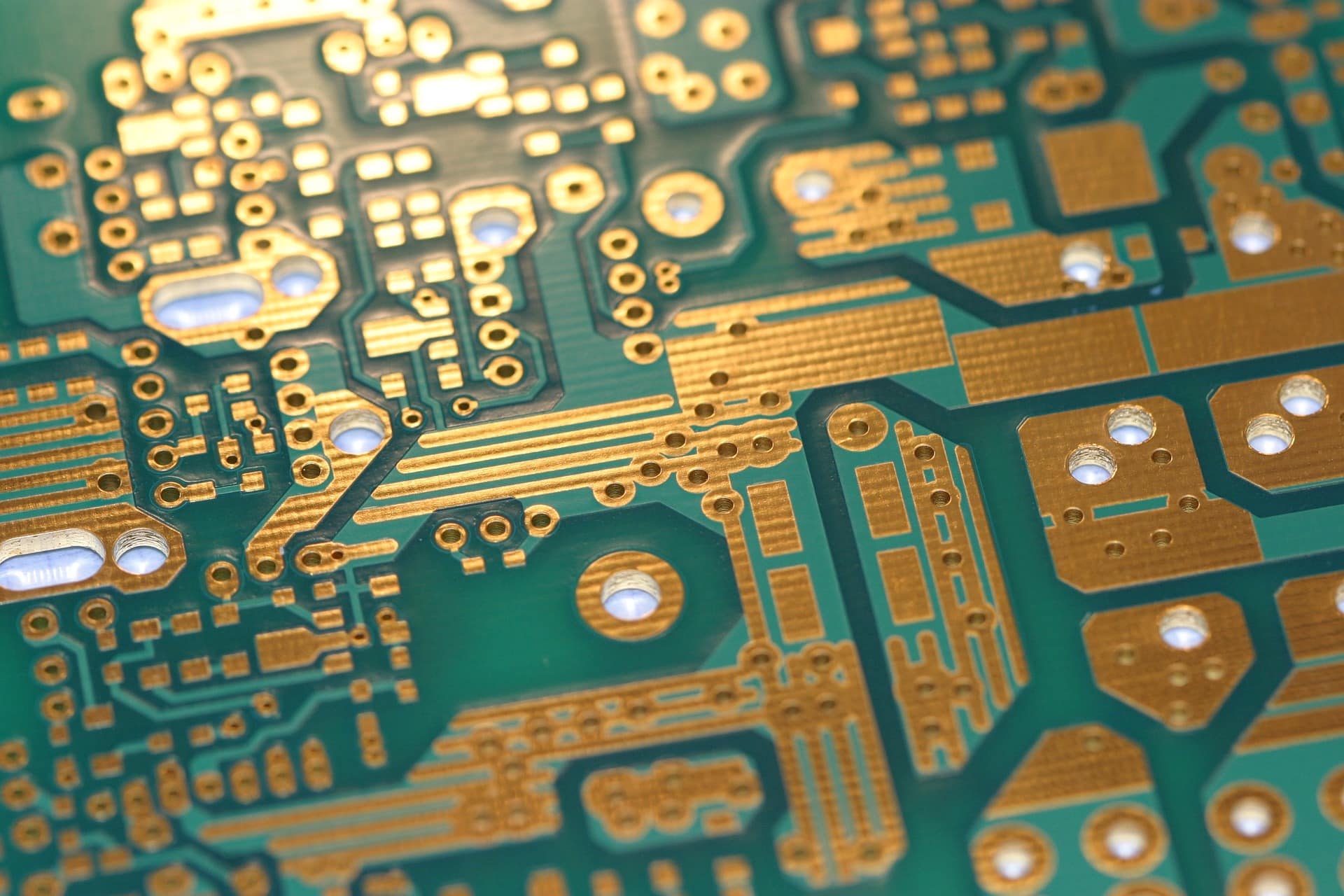
PCB厂:基于Cadence的高速PCB设计分享 - 鑫景福科技
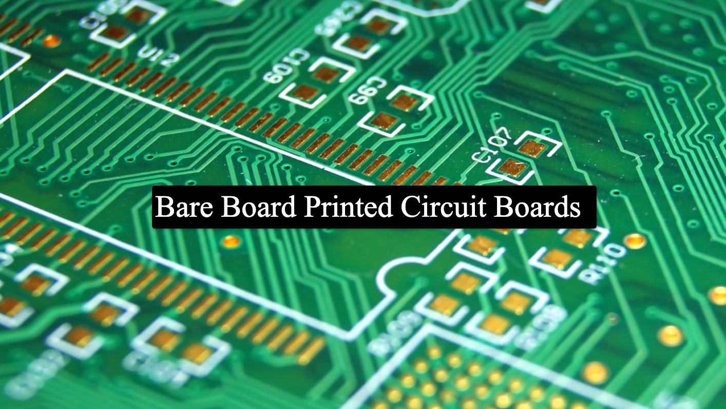
Bare Board Printed Circuit Boards - Bare Board PCBs - AES
 absolutepcbassembly.com
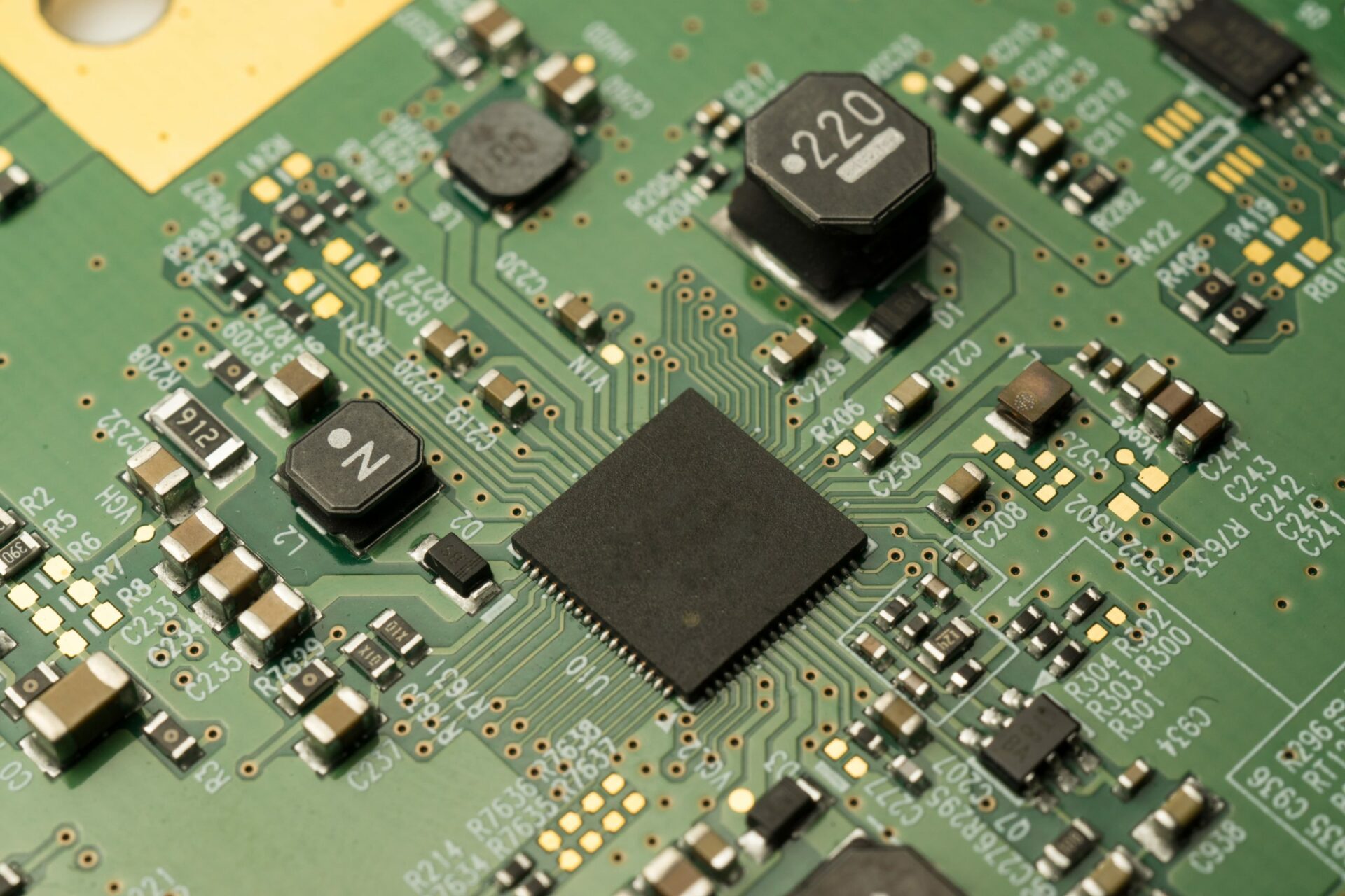
Bare Board Printed Circuit Boards - Bare Board PCBs - AES
Pengertian PCB (Printed Circuit Board) : Jenis Dan Fungsinya Secara Lengkap
 www.bengkeltv.id
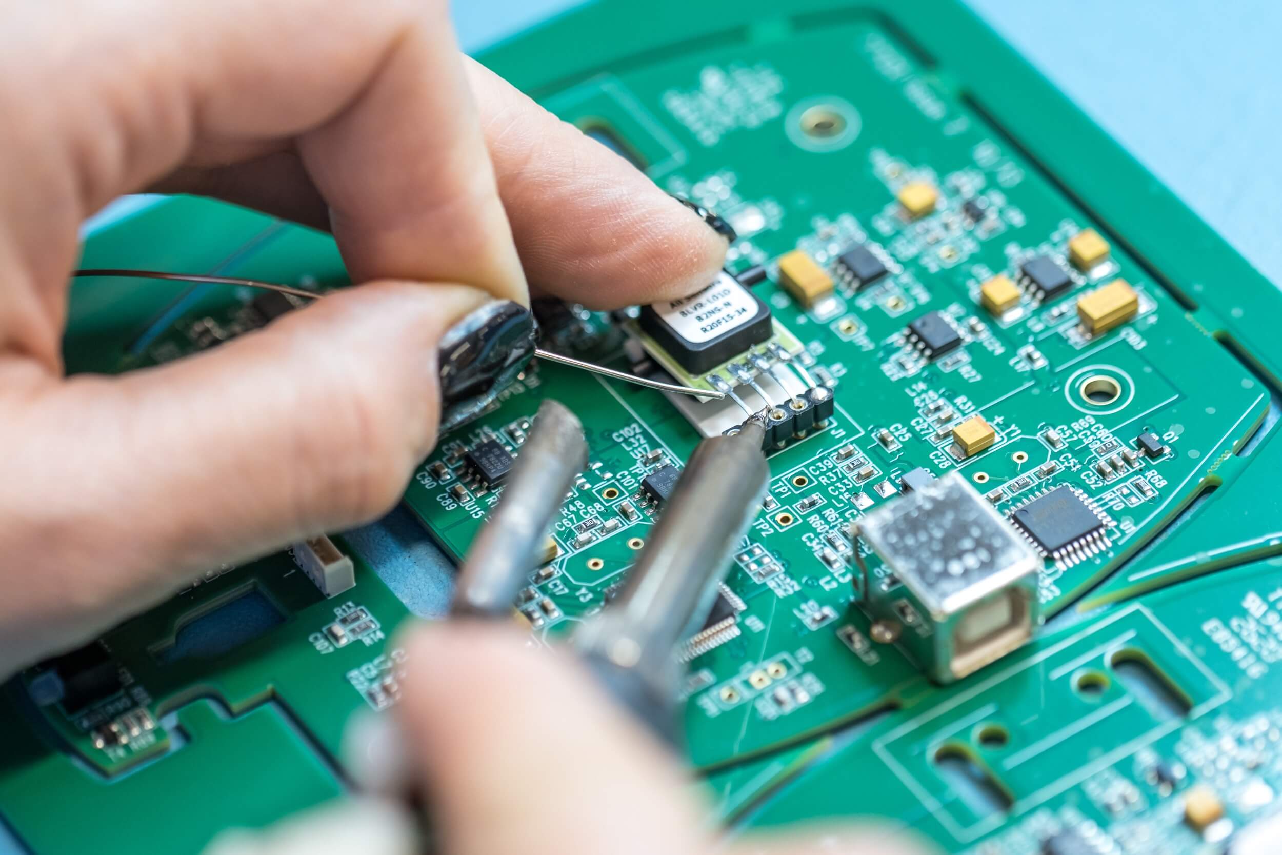
Pengertian PCB (Printed Circuit Board) : Jenis dan Fungsinya Secara Lengkap
Printed Circuit Board (PCB) Design Service - CIRCUITSTATE Electronics
 www.circuitstate.com
Printed Circuit Board (PCB) Design Service - CIRCUITSTATE Electronics
What Is IC PCB Board? – Hillman Curtis: Printed Circuit Board
 hillmancurtis.com
What is IC PCB Board? – Hillman Curtis: Printed Circuit Board ...
Mastering The Art Of PCB Design Basics | Sierra Circuits
 www.protoexpress.com
Mastering the Art of PCB Design Basics | Sierra Circuits
Printed Circuit Boards (PCBs): Ultimate Guide | Reversepcb
 reversepcb.com
Printed Circuit Boards (PCBs): Ultimate Guide | Reversepcb
Your Guide To Working With A High Density PCB – Hillman Curtis: Printed
 hillmancurtis.com
Your Guide to Working with a High Density PCB – Hillman Curtis: Printed ...
Factors That Influence Custom PCB Cost – Hillman Curtis: Printed
 hillmancurtis.com
Factors That Influence Custom PCB Cost – Hillman Curtis: Printed ...
Printed Circuit Board Assembly Services | Technical Specification
 www.hemeixinpcb.com
Printed Circuit Board Assembly Services | Technical specification
PCB Manufacturing Process [Step-by-Step Guide]
![PCB Manufacturing Process [Step-by-Step Guide]](https://www.cirexx.com/wp-content/uploads/pcb-manufacturing-process-1024x682.jpg) www.cirexx.com
www.cirexx.com
PCB Manufacturing Process [Step-by-Step Guide]
5 Types Of PCB Surface Finishing
 blog.techdesign.com
5 Types of PCB Surface finishing
PCB Assembly UK | PCBA | ABL Circuits
 www.ablcircuits.co.uk
PCB Assembly UK | PCBA | ABL Circuits
A Brief Guide To PCB Assembly Services
 aaloktronix.com
A Brief Guide to PCB Assembly Services
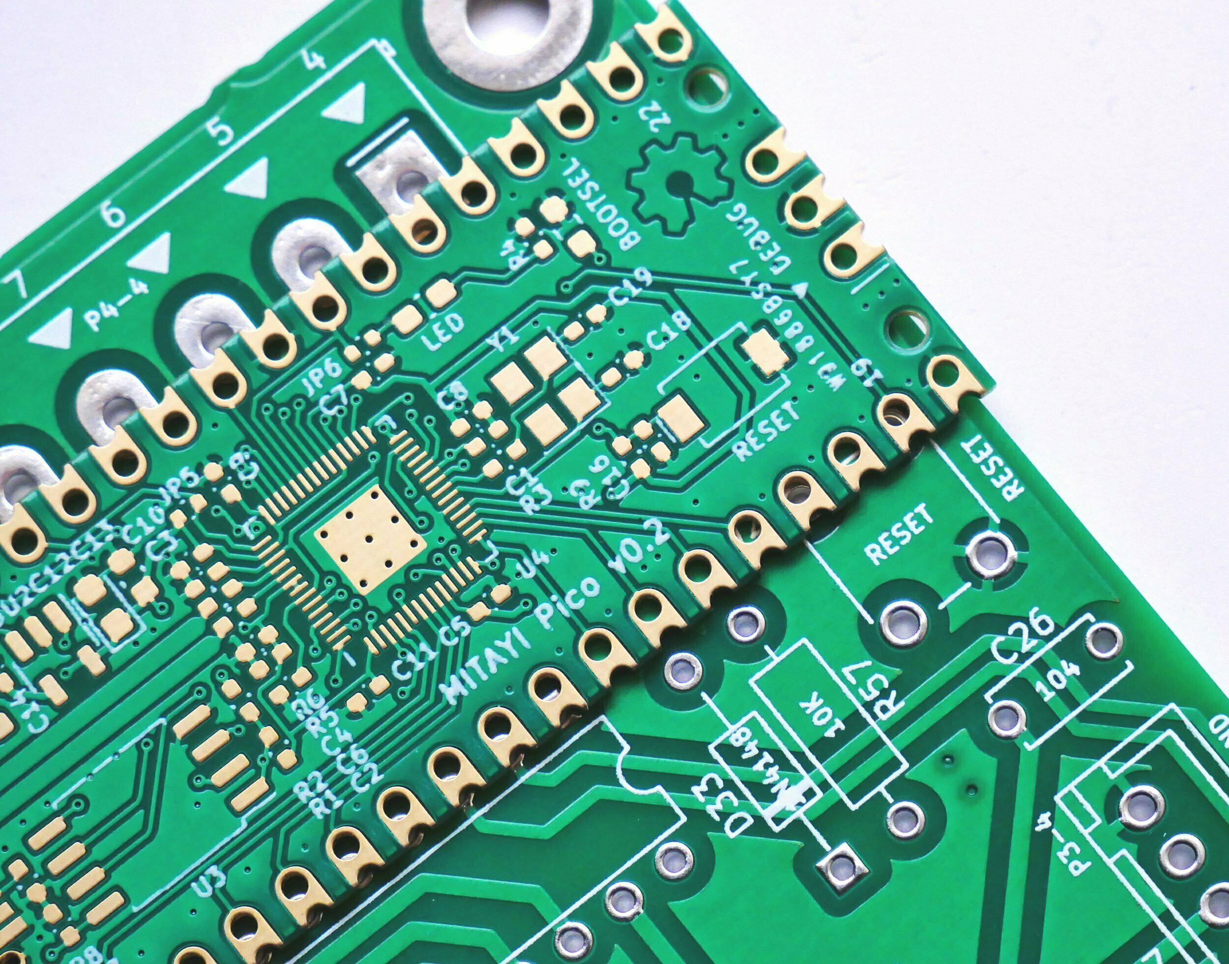
Blank PCB Board: Its Usage And Usefulness – Hillman Curtis: Printed
 hillmancurtis.com
Blank PCB Board: Its Usage and Usefulness – Hillman Curtis: Printed ...
All About Printed Circuit Board (PCB) | Multi-Teknik
 www.multekpcb.com
All About Printed Circuit Board (PCB) | Multi-Teknik
Failure Checking Method On Newly Designed PCB Board – PCB Manufacturing
 www.grande-pcba.com
Failure Checking Method On Newly Designed PCB Board – PCB Manufacturing ...
Designing High-Performance PCB Circuit Boards: Key Tips - PCB And Assembly
 pcbandassembly.com
Designing High-Performance PCB Circuit Boards: Key Tips - PCB And Assembly
Pcb Design And Fabrication Schematic Diagram To Pcb Layout
 pcbways.pages.dev
pcb design and fabrication Schematic diagram to pcb layout
PCB Trace: The Backbone Of Modern Circuit Design
 www.wevolver.com
PCB Trace: The Backbone of Modern Circuit Design
Pcb Schematic And Layout How To Design A Pcb Layout
 babogediboplibguide.z13.web.core.windows.net
Pcb Schematic And Layout How To Design A Pcb Layout
PCB (Printed Circuit Board) : PCB Designing, Manufacturing And Assembly
 www.electronicsandyou.com
PCB (Printed Circuit Board) : PCB Designing, Manufacturing and Assembly
Pcb Course Class 11 Images 94v Circuit Diagram - Elara Orla
 elaraorla.pages.dev
pcb course class 11 images 94v Circuit Diagram - Elara Orla
All About Printed Circuit Board (PCB) | Multi-Teknik
 www.multekpcb.com
All About Printed Circuit Board (PCB) | Multi-Teknik
PCB Meaning In Electronics | Video& Image& Text Explanation
 www.fs-pcba.com
PCB Meaning in Electronics | Video& Image& Text Explanation
Your guide to working with a high density pcb – hillman curtis: printed. pcb厂:基于cadence的高速pcb设计分享. pcb schematic and layout how to design a pcb layout